← Back
Article image
πŸ“° News ⏱ 2 min
πŸ”‘

Key Points

5 points
1

Semicon 2.0 budget: ₹127,500 crore

2

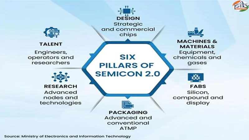
Six strategic areas: research, design, machines & materials, new fabrication plants, advanced packaging, talent

3

Goal: cover whole value chain from silicon material to finished chip systems

4

India currently hosts about 7 % of global semiconductor design centres and 20 % of design workforce

5

Key applications include smartphones, autonomous vehicles, satellites and defence systems

πŸ“–

Summary

The initiative builds on Semicon 1.0 and adds focus on research, design tools, advanced packaging, specialised equipment and skilled workforce development.

India aims to reduce reliance on imports, support sectors such as smartphones, electric vehicles, space missions and Artificial Intelligence.

Projected chip demand could reach $110 billion by 2030, prompting investment in 12 manufacturing units and thousands of design projects.

International partnerships with the United States, Japan, Europe and others will complement the domestic effort.

πŸ“˜

New Words to Learn

9 words
ecosystem
All the different parts that work together, like factories, schools and companies
value chain
The series of steps that turn raw material into a finished product
fabrication plant
A large factory where chips are made
nanometer
A unit of length that is one‑billionth of a meter, used to describe tiny chip features
compound semiconductor
A chip made from a mix of two or more elements, giving special properties
radiation‑hardened
Designed to keep working even in the strong radiation of space
Analog‑to‑Digital Converter
A device that changes real‑world signals into numbers a computer can understand
strategic
Very important for a country's plans and safety
resilience
The ability to keep working even when problems happen
πŸ”— Read Full Article β†’

Want to learn even more? Click here to read the full story!

πŸ”Š Reading Article
Kid-friendly voice
πŸ†

New Badge Unlocked!

Badge Name
Badge description